The sensor is the soul of your digital camera and knowing
how it works will help you to compose better images
By Michael Guncheon
Sophisticated technology
goes into the design and manufacture of your digital camera.
Understanding some of that technology can help you to predict
how the camera will fare when you’re shooting in a variety
of situations. For our annual How-To issue, we’re including
this article on the anatomy of an image sensor. The overall
image quality in your photographs is dependent upon a number
of factors in addition to sensor resolution. Lens quality, in-camera
processing, compression algorithms and just plain old shooting
technique all work together. Still, the image sensor is the
core around which the rest of the camera is built.
Much more than a
simple replacement of film, the sensor is a high-tech piece
of electronic wizardry. There are two types of image sensors
used in today’s digital cameras: charge-coupled devices
(CCDs) and CMOS chips, which is an acronym for complementary
metal-oxide semiconductor. The names don’t help to explain
what they do. CCD refers to the design of the chip, and CMOS
refers to the chip’s manufacturing process. While the vast
majority of image sensors are CCDs, both of the devices are
designed to achieve the same result: converting light into an
electrical charge. And although both devices are made of silicon,
it’s how they operate that differentiates them.
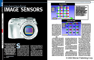
CCD
Let’s examine how CCDs operate. The CCD is comprised of
a series of photosites in a grid pattern. Each photosite contains
a light-sensing device (a photodiode) and a storage area to
hold the charge created by the photodiode. When light hits the
photodiode, it converts the light into electrons, or a charge.
The more light that hits the photodiode, the greater the charge.
The next step in the process is to move the charge out of the
photosites and into another area of the chip called a transfer
register. Row by row, each row of charges is moved vertically
and passed into the transfer register. When a row reaches the
transfer register, the photosite charges are read out (horizontally)
one by one, converted into a voltage and amplified. Once one
row has been read out, its charges are deleted and the next
row drops down into its place to be read out. This coupling
of one row to the next is where the device gets its name. Further
processing of the signal is required to convert the analog voltage
into a digital signal. This A-to-D processing is done on a separate
chip.
In order to sample the color information of the light hitting
the photodiodes, a series of filters are embedded into the chip
so that some photosites are reading red light, some blue and
others green.
CMOS
Now let’s look at a CMOS. Like a CCD, a CMOS image sensor
is also comprised of a series of photosites arranged in a grid
pattern; however, the makeup of each photosite differs from
the CCD. A CMOS photosite contains a photodiode for converting
photons or light to electrons, but rather than storing the charge
and processing the data in another part of the chip (or even
outside of the chip), some of the processing is done at the
photosite itself. Each photosite contains a converter for changing
the charge to a voltage, an amplifier to increase the very low
signal coming from the photodiode, and circuitry to reduce noise
in the signal. There’s a series of grid connections among
the photosites in order to read out the data, and while they
might be arranged in rows and columns, the design allows for
accessing each photosite directly as opposed to reading out
row by row.
As far as sampling the color information, with most CMOS image
sensors, a similar technique to the CCD is used to filter the
photosites so that they receive the appropriate colors of light.
One manufacturer, Foveon, uses the properties of silicon itself
to filter out the various colors of light. This process allows
each photosite to capture red, green and blue rather than just
one color. (The Foveon image sensor is currently only available
on Sigma digital SLRs, but we expect to see other camera manufacturers
employing the sensor in the future.)
Comparing Design Differences
So how do these design differences compare? Let’s break
it down into a few specific topics.
Power Consumption. It turns
out that in order to read out all of that data from the photosites
in a row-by-row and then pixel-by-pixel fashion in a CCD, there
are all sorts of sophisticated timing signals that need to be
generated. And while it’s technically possible to put all
of those timing generators and other necessary processing functions
on the CCD, it’s not very economical to do so.
With a CMOS image sensor, many of the processing functions can
be built into the chip during manufacture much like Pentium
CPUs have onboard memory built right into the chip. So a CCD
requires additional integrated circuit chips compared to a CMOS
image sensor in order to process the data. Anytime you add circuitry,
you add power consumption. Therefore, a CCD will consume more
power than a CMOS image sensor.
Speed. By having to shift
charges around the CCD and parse out the data one row at a time,
a CCD can take a long time to create an entire image. With the
CMOS sensor having individual charge converters and amplifiers
in each photosite, the whole image can be read out much faster.
Yet another speed increase is found with the CMOS sensor if
you use special capture functions that utilize only a part of
the sensor. Let’s say that you’re capturing an image
using only one half of the sensor. Since the CMOS chip can access
only the pixels it needs, the frame rate of the image capture
is increased. With a CCD, even if you’re only using the
middle part of the sensor, the chip still has to shift the data
from all the photosite rows, one by one, until it gets the data
it needs.
Sensitivity. If you examine
each photosite of a CMOS, you’ll see that the power-saving
and speed-enhancing circuitry of converters and amplifiers takes
up space. That extra space can’t be used for capturing
light. On the other hand, a CCD sensor might capture 100 percent
of the light hitting the photosite.
Noise. CCDs essentially have
a single amplifier through which all of the data travels. That
and the fact that extra processing is done off the image sensor
means the noise on a CCD is largely kept at bay.
A CMOS chip may contain millions of tiny converters and amplifiers
in each photosite. In a perfect world, all of those converters
and amplifiers would work exactly alike, no matter the operating
environment. But this isn’t a perfect world. As all of
the amplifiers begin working at different efficiencies, they
induce fixed-pattern noise into the data that they’re amplifying.
(What’s fixed-pattern noise? Imagine taking a picture with
the lens cap on and having some of the pixels register black
and some register a little lighter than black. That’s an
approximation of fixed-pattern noise.) Also, having that additional
circuitry all on the same chip can add noise.
Blooming. Blooming occurs
when the electron charge leaks from one photosite to the other.
It can be seen in the image as streaks anchored at small high-brightness
areas. CCDs are prone to blooming when individual photosites
are oversaturated.
Since CMOS sensors convert the charge to a voltage right at
the photosite, it’s more difficult for the charge to leak
to adjacent photosites. CMOS chip builders also can add pixel-reset
circuitry right at the photosite to minimize overloading (remember
all that extra circuitry they can add directly to the photosite?).
So by its inherent design, CMOS sensors generally are immune
to blooming.
Of course, the question is, Which sensor is better? It’s
an impossible question to answer definitively. Obviously, there
are pluses and minuses with each technology, but the manufacturers
aren’t ignoring these differences. For example, CCD designers
have gone to different read-out methods such as reading out
the entire sensor at once in order to increase speed, while
CMOS designers may incorporate special noise-reduction circuitry
to reduce photosite noise, or they may add lenses to the individual
photosites to increase sensitivity. CMOS chips also are being
produced with more on-chip functions that take advantage of
the flexibility of CMOS technology.
Although the image sensor is the heart of the digital camera,
there’s more to a digital camera than just the sensor.
The data coming out of the chip needs extensive processing to
achieve an image to store on the media card. Image-processing
software algorithms are sophisticated custom software embedded
into the camera to minimize the minuses and take advantage of
the pluses of the image sensors.
Much like you wouldn’t buy a car based only on the engine
under the hood, you wouldn’t want to decide on a camera
without considering the whole picture.